Nanogap fabrication
Light-matter interaction at the nanoscale is one of the most focused research areas in our group. In this regard, nanofabrication becomes a vital component of our laboratory. A novel fabrication technique called “Atomic Layer Lithography (ALD)” was developed, which combines lithography with atomic layer deposition of alumina to create nanogap with an unprecedented width resolution towards ~1 nm. We could have also developed a technique to fabricate samples with sub-nm width (~3 Å) by using graphene as a spacer (van-der Waals gap).
We are also developing samples with the ability to control the gap-width actively from quantum to classical scale by using external stimuli such as strain, electrically, temperature. We developed “Zero-Nanometer-Gap (zero-gap)” technology and “Closable-Gap” which enables us to control the gap width on an unprecedented scale from quantum to nano to classical gap and vice versa.
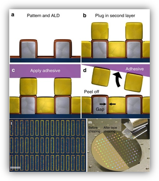
Atomic layer lithography
Nature Communications 4, 2361 (2013)
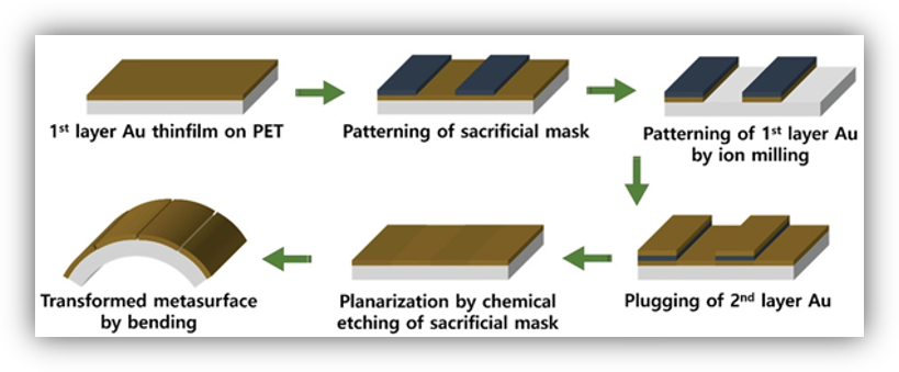
Zero-nanometer gap technology
Adv. Opt. Mater., 2002164 (2021)
Nano Lett. 21, 4202-4208